
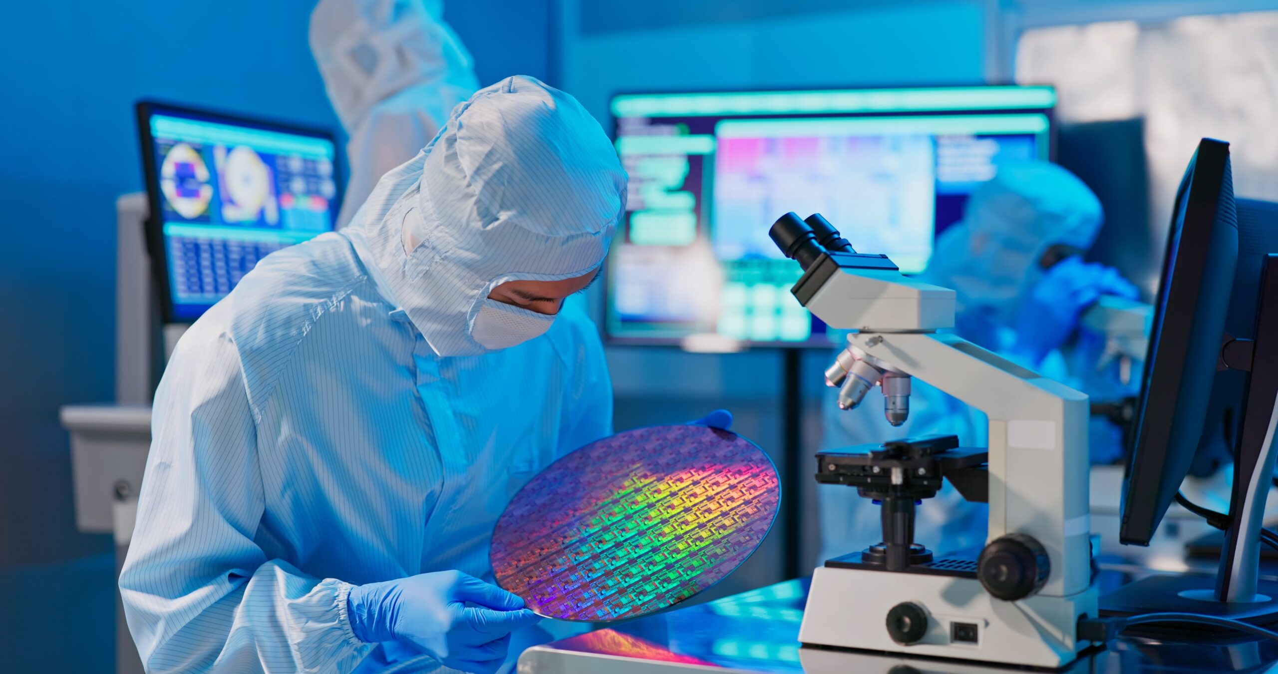
MicroLED Inspection & Testing for AR & Smart Glasses
AR microdisplays are comprised of single µm chips, and demand extremely high luminance with flawless uniformity. InZiv enables sub-micron, wafer-level insight – before costly assembly.
For Clarity, Compactness & Control
Near-eye AR requires very high pixel density and very high luminance to the eye, while staying lightweight and efficient. MicroLED chips in micro-displays (typically on CMOS backplanes) are used because they can deliver high brightness, high efficiency, and the necessary small form factor.

MicroLED Challenges for AR & Smart Glasses
As pixel sizes shrink and brightness requirements soar, every imperfection and color shift matters.
Microscopic Pixels, Magnified Defects
Tiny pixels (≈1–5 µm) magnify the impact of minute defects on uniformity and maintaining high EQE is a greater challenge the smaller the die.
Extreme Brightness, Extreme Stress
High luminance requirements (often tens to hundreds of thousands of nits at the panel level, in order to achieve hundreds of nits to the eye through optics) raise thermal/electrical stress and color shift risks.
Sub-Pixel Color Complexity
Complex color formation (e.g., QD color conversion on blue µLEDs) adds additional uniformity and efficiency variables at the sub-pixel level.
InZiv’s Solutions
InZiv provides a comprehensive inspection and metrology solution for microLEDs, spanning in-depth characterization, high-throughput data collection, and production-level inspection.
microLED Production at Scale
R-EL Glide
Provides high-throughput EL inspection up to 6M LEDs/hour with true EL contact for accurate electrical testing without damaging devices.
Automated wafer handling, alignment, and probe card replacement streamline production and enable yields compatible with mass manufacturing.


Turn-Key Metrology for R&D
OmniPix 3.0
Delivers nano-EL/PL resolution down to 100 nm, enabling inspection of pixels as small as 1 µm, with spectral resolution <1 nm for tight wavelength binning.
The thermal chuck (10–100 °C) allows stress testing under realistic operating conditions, while angular emission mapping (±70°, 1° resolution) captures the optical profile critical to AR optics.
Why It Matters
Early, wafer-level detection/repair improves yield and shortens time-to-integration for AR optical engines—where brightness, size, and uniformity are unforgiving.
Industry demonstrations already show microLED microdisplays achieving hundreds of thousands to millions of nits, underscoring the need for robust metrology.

Technical Specifications
The table below outlines representative performance targets used to illustrate inspection challenges; actual requirements vary by application and system design.
| Parameter | Example Performance Requirement | How InZiv Measures & Enables |
|---|---|---|
| Pixel size | ~1–5 µm | OmniPix 3.0 measures chips as small as 1 µm, with nano-EL/PL resolution down to 100 nm. |
| Brightness | 500k–1M nits at panel | OmniPix maps PL/EL intensity and EQE; thermal chuck (10–100 °C) ensures stability testing. |
| Color uniformity | Δu’v’ <0.01 | Spectral resolution <1 nm (400–800 nm) allows precise wavelength uniformity mapping. |
| Defect detection | Sub-pixel mura, dead pixels | Nano-EL/PL with angular measurements (±70°, 1° res) detects structural correlations. |

GET A CLOSER LOOK
See InZiv in Action
The future of microLED begins with InZiv.
We would be happy to schedule a confidential call to discuss your specific needs and answer your questions. We can also provide a confidential demonstration of InZiv’s testing and inspection technology on your sample.
Discover the technology powering the next generation of microLED displays.
