
MicroLED Inspection & Testing for Tiled TVs & Signage
Seamless walls start with perfect wafers. Large-area microLED TVs are modular and bright. InZiv helps ensure the tiles look like one flawless panel.
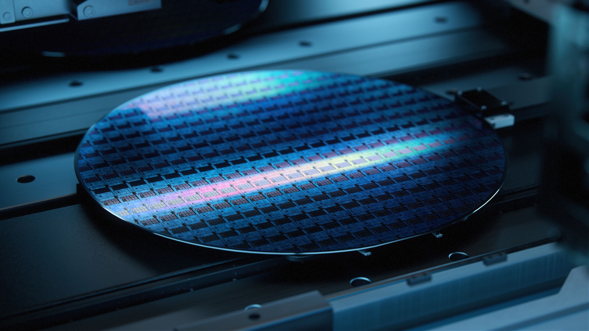
For Massive Scale & Pixel Perfection
MicroLED TVs and large signage displays are built from modular tiles, allowing seamless walls that scale to any size. Each tile contains millions of emitters that must be perfectly uniform to avoid visible seams. Commercial models already demonstrate ~2,000 nit peak brightness with superior lifetime and thermal stability compared to OLED. Achieving consumer-ready performance requires tight wavelength binning, luminance uniformity, and extremely low defectivity across billions of pixels.

MicroLED Challenges for TVs and Signage
At large scales and high resolutions, microLED displays demand exceptional pixel-to-pixel uniformity, precise color control, and manufacturability across millions of emitters.
Uniformity Across Tiles
Small wavelength/brightness variation becomes visible in large walls; origin is frequently wafer-level emitter variability.
Brightness Stability
Even at high drive, devices must demonstrate luminance stability (window-facing installs often need higher nits).
Mass Transfer Yield
Billions of emitters across tiles—detection and repair are essential.
InZiv’s Solutions
InZiv provides a comprehensive inspection and metrology solution for microLEDs, spanning in-depth characterization, high-throughput data collection, and production-level inspection.
MicroLED Production at Scale
R-EL Glide
Provides true EL-based inspection at industrial throughput (up to 6M LEDs/hour) to catch and localize defective emitters before dicing and module assembly.
The system delivers wavelength, intensity, and IV data per device with automated pass/fail classification, improving effective yields.


Turn-Key Metrology for R&D
OmniPix 3.0
Maps wafer-level wavelength and luminance distributions with <1 nm spectral resolution, supporting narrow binning windows required for seamless tile-to-tile matching.
Angular emission mapping (±70°) helps ensure consistent brightness and color uniformity across large-format modular displays.
Nano-EL/PL at 100 nm resolution detects sub-micron defects in 20–50 µm emitters typical of TV-class dies.
Why It Matters
The business case for microLED TVs and outdoor signage hinges on yield, repair, and uniformity.
Upstream metrology is the lever that makes modular panels look truly seamless, at consumer-viable costs.

Technical Specifications
The table below outlines representative performance targets used to illustrate inspection challenges; actual requirements vary by application and system design.
| Parameter | Example Performance Requirement | How InZiv Measures & Enables – Examples |
|---|---|---|
| Die size | 20–50 µm | OmniPix accommodates multiple wafer sizes (coupon–8″) and chip architectures. |
| Pixel pitch | 0.6–1.2 mm | Full-wafer PL/EL maps ensure uniform tile performance. |
| Peak brightness | Up to 4,000 nits | OmniPix measures EL intensity distribution; R-EL Glide ensures defect-free tiles. |
| Tile uniformity | <2 nm wavelength / <3% luminance variation | Spectral resolution <1 nm and automated wafer mapping enable tight binning. |

GET A CLOSER LOOK
See InZiv in Action
The future of microLED begins with InZiv.
We would be happy to schedule a confidential call to discuss your specific needs and answer your questions. We can also provide a confidential demonstration of InZiv’s testing and inspection technology on your sample.
Discover the technology powering the next generation of microLED displays.
